 | –≠–ª–µ–∫—Ç—Ä–æ–Ω–Ω—ã–π –∫–æ–º–ø–æ–Ω–µ–Ω—Ç: AN8004 | –°–∫–∞—á–∞—Ç—å:  PDF PDF  ZIP ZIP |
s Overview
The AN8000 series is 3-pin low-dropout fixed positive
output monolithic voltage regulators. Since thier power
consumption can be minimized, they are suitable for bat-
tery stabilizing power supply and reference voltage. Thir-
teen types of output voltage are available ; 2V, 2.5V, 3V,
3.5V (TO-92 only) , 4V, 4.5V, 5V, 6V, 7V, 8V, 8.5V, 9V,
and 10V.
s Features
∑ Input/output voltage difference : 0.3V
(
max.
)
∑ Output current of up to 50mA
∑ Low bias current ; 0.6mA
(
typ.
)
∑ Output voltage ; 2V, 2.5V, 3V, 3.5V (TO-92 only) , 4V,
4.5V, 5V, 6V, 7V, 8V, 8.5V, 9V, and 10V.
∑ Over-voltage protective circuit built-in.
AN8000/AN8000M Series
3-pin Positive Output Low Dropout Voltage Regulator (50mA Type)
s Block Diagram
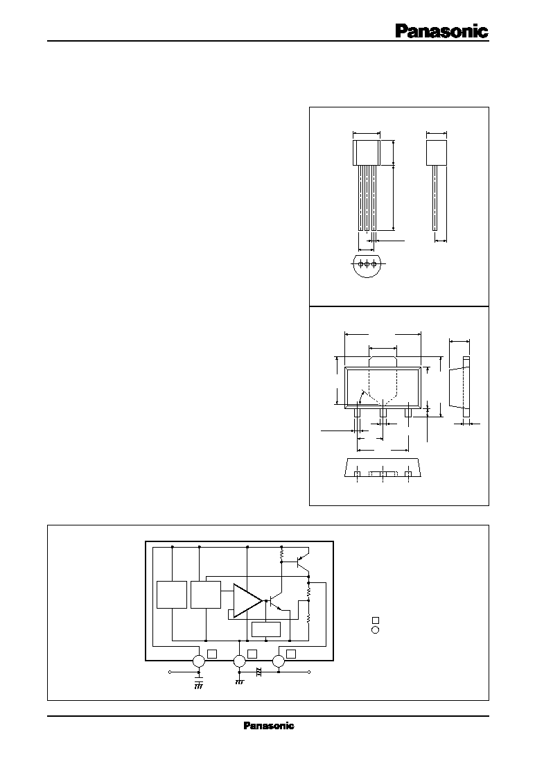
Unit:mm
AN8000 Series
5.0
±
0.2
TO-92 Plastic Package (SSIP003-P-0000)
5.1
±
0.2
13.5
±
0.5
0.45
2.3
±
0.2
2.54
(Bottom View)
3
2
1
+ 0.2
≠ 0.1
4.0
±
0.2
1 : Input
2 : Output
3 : GND
2.6
45∞
1.6max.
1.8max.
3.0
1.5
1
2
3
0.48max.
0.58max.
3-pin Mini Power type Plastic Package (TO-243) (HSIP003-P-0000B)
0.44max.
4.25max.
2.6max.
0.8min.
Unit:mm
AN8000M Series
4.6max.
1 : Output
2 : GND
3 : Input
Voltage
Reference
Current
Limiter
Starter
V
O
R
1
R
2
C
OUT
R
1
=5k
C
IN
=0.33
µ
F
C
OUT
=10
µ
F
V
I
2
3
1
: TO-92
: TO-243
+
Error
Amp.
≠
1
2
3
≠
+
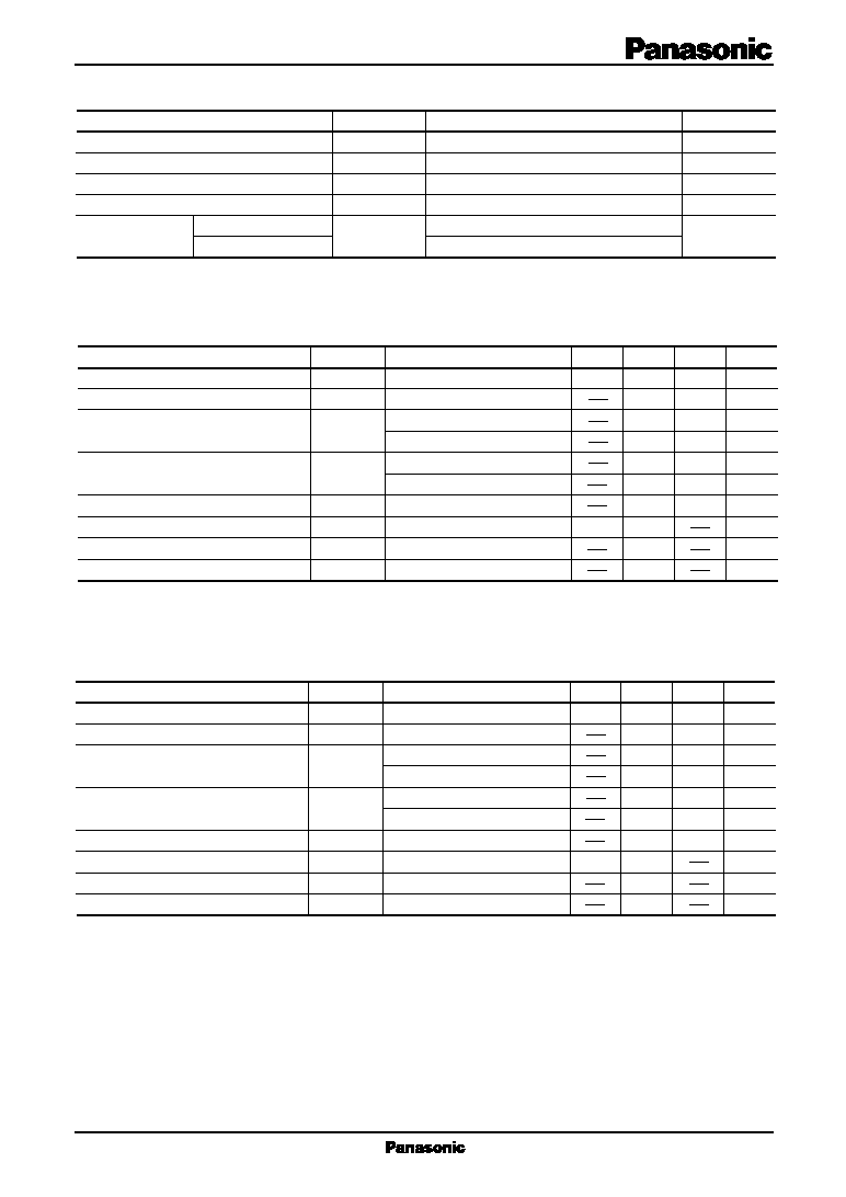
V
I
I
CC
P
D
T
opr
T
stg
Supply voltage
Supply current
Power dissipation
Operating ambient temperature
Storage temperature
Parameter
Symbol
Rating
s Absolute Maximum Ratings (Ta=25∞C)
20
100
650 *
≠30 to+80
≠55 to+150
≠55 to+125
* Mounting onto the PCB (20
◊
20
◊
1.7mm glass epoxy copper foil 1 cm
2
or more), for AN8000M Series.
AN8000 Series
AN8000M Series
V
mA
mW
∞C
∞C
Unit
Parameter
Symbol
Condition
min
typ
max
Output voltage
V
O
2.08
V
2
Line regulation
REG
IN
mV
Load regulation
REG
L
20
mV
mV
Minimum I/O voltage difference
V
0.06
V
mA
0.6
Bias current
I
bias
dB
Ripple rejection ratio
RR
Output noise voltage
V
no
0.1
Output voltage temperature coefficient
25
40
0.2
0.3
1
1.92
62
0.12
2
7
10
60
74
Unit
T
j
=25∞C
V
I
=2.5 to 8V, T
j
=25∞C
I
O
=1 to 40mA, T
j
=25∞C
V
DIF (min.)
V
I
=1.9V, I
O
=20mA, T
j
=25∞C
V
I
=1.9V, I
O
=50mA, T
j
=25∞C
I
O
=1 to 50mA, T
j
=25∞C
I
O
=0mA, T
j
=25∞C
Note1) The specified condition T
j
=25∞C means that the test should be conducted with each test time reduced (within 10ms) so that
the drift in characteristic value due to a temperature rise at chip junction can be ignored.
Note2) Unless otherwise specified, V
I
=3V, I
O
=20mA, C
O
=10
µ
F
V
I
=3 to 5V, f=120Hz
µ
V
mV/∞C
f=10Hz to 100kHz
V
O
/Ta
T
j
=≠30 to+125∞C
s Electrical Characteristics (Ta=25∞C)
∑
AN8002/AN8002M (2V Type)
T
j
=25∞C
V
I
=3 to 8.5V, T
j
=25∞C
I
O
=1 to 40mA, T
j
=25∞C
V
DIF (min.)
V
I
=2.4V, I
O
=20mA, T
j
=25∞C
V
I
=2.4V, I
O
=50mA, T
j
=25∞C
I
O
=1 to 50mA, T
j
=25∞C
I
O
=0mA, T
j
=25∞C
Note1) The specified condition T
j
=25∞C means that the test should be conducted with each test time reduced (within 10ms) so that
the drift in characteristic value due to a temperature rise at chip junction can be ignored.
Note2) Unless otherwise specified, V
I
=3.5V, I
O
=20mA, C
O
=10
µ
F
V
I
=3.5 to 5.5V, f=120Hz
µ
V
V
no
mV/∞C
f=10Hz to 100kHz
V
O
/Ta
T
j
=≠30 to+125∞C
∑
AN8025/AN8025M (2.5V Type)
V
O
2.6
V
2.5
REG
IN
mV
REG
L
20
mV
mV
V
0.07
V
mA
0.6
I
bias
dB
RR
V
no
0.13
25
50
0.2
0.3
1
2.4
60
0.12
2.5
8
12.5
65
72
Parameter
Symbol
Condition
min
typ
max
Unit
Output voltage
Line regulation
Load regulation
Minimum I/O voltage difference
Bias current
Ripple rejection ratio
Output noise voltage
Output voltage temperature coefficient

V
O
3.12
V
3
T
j
=25∞C
REG
IN
mV
V
I
=3.5 to 9V, T
j
=25∞C
REG
L
25
mV
I
O
=1 to 40mA, T
j
=25∞C
mV
V
DIF (min.)
V
0.07
V
I
=2.9V, I
O
=20mA, T
j
=25∞C
V
V
I
=2.9V, I
O
=50mA, T
j
=25∞C
I
O
=1 to 50mA, T
j
=25∞C
mA
0.6
I
O
=0mA, T
j
=25∞C
Note1) The specified condition T
j
=25∞C means that the test should be conducted with each test time reduced (within 10ms) so that
the drift in characteristic value due to a temperature rise at chip junction can be ignored.
Note2) Unless otherwise specified, V
I
=4V, I
O
=20mA, C
O
=10
µ
F
I
bias
dB
V
I
=4 to 6V, f=120Hz
RR
µ
V
V
no
mV/∞C
0.15
f=10Hz to 100kHz
V
O
/Ta
T
j
=≠30 to+125∞C
30
50
0.2
0.3
1
2.88
58
0.12
3
9
15
70
70
Parameter
Symbol
Condition
min
typ
max
Output voltage
Line regulation
Load regulation
Minimum I/O voltage difference
Bias current
Ripple rejection ratio
Output noise voltage
Output voltage temperature coefficient
Unit
∑
AN8003/AN8003M (3V Type)
s Electrical Characteristics (Ta=25∞C)
T
j
=25∞C
V
I
=4.5 to 10V, T
j
=25∞C
I
O
=1 to 40mA, T
j
=25∞C
V
DIF (min.)
V
I
=3.8V, I
O
=20mA, T
j
=25∞C
V
I
=3.8V, I
O
=50mA, T
j
=25∞C
I
O
=1 to 50mA, T
j
=25∞C
I
O
=0mA, T
j
=25∞C
Note1) The specified condition T
j
=25∞C means that the test should be conducted with each test time reduced (within 10ms) so that
the drift in characteristic value due to a temperature rise at chip junction can be ignored.
Note2) Unless otherwise specified, V
I
=5V, I
O
=20mA, C
O
=10
µ
F
V
I
=5 to 7V, f=120Hz
µ
V
V
no
mV/∞C
f=10Hz to 100kHz
V
O
/Ta
T
j
=≠30 to+125∞C
∑
AN8004/AN8004M (4V Type)
V
O
4.16
V
4
REG
IN
mV
REG
L
30
mV
mV
V
0.07
V
mA
0.6
Parameter
Symbol
Condition
min
typ
max
Output voltage
Line regulation
Load regulation
Minimum I/O voltage difference
Bias current
Ripple rejection ratio
Output noise voltage
Output voltage temperature coefficient
Unit
I
bias
dB
RR
V
no
0.2
40
50
0.2
0.3
1
3.84
56
0.12
3.5
10
20
80
67
T
j
=25∞C
V
I
=4 to 9.5V, T
j
=25∞C
I
O
=1 to 40mA, T
j
=25∞C
V
DIF (min.)
V
I
=3.4V, I
O
=20mA, T
j
=25∞C
V
I
=3.4V, I
O
=50mA, T
j
=25∞C
I
O
=1 to 50mA, T
j
=25∞C
I
O
=0mA, T
j
=25∞C
Note1) The specified condition T
j
=25∞C means that the test should be conducted with each test time reduced (within 10ms) so that
the drift in characteristic value due to a temperature rise at chip junction can be ignored.
Note2) Unless otherwise specified, V
I
=4.5V, I
O
=20mA, C
O
=10
µ
F
V
I
=4.5 to 6.5V, f=120Hz
µ
V
V
no
mV/∞C
f=10Hz to 100kHz
V
O
/Ta
T
j
=≠30 to+125∞C
∑
AN8035/AN8035M (3.5V Type)
V
O
3.64
V
3.5
REG
IN
mV
REG
L
30
mV
mV
V
0.07
V
mA
0.6
I
bias
dB
RR
V
no
0.2
40
50
0.2
0.3
1
3.36
57
0.12
3.5
10
20
75
69
Parameter
Symbol
Condition
min
typ
max
Output voltage
Line regulation
Load regulation
Minimum I/O voltage difference
Bias current
Ripple rejection ratio
Output noise voltage
Output voltage temperature coefficient
Unit
T
j
=25∞C
V
I
=5 to 10.5V, T
j
=25∞C
I
O
=1 to 40mA, T
j
=25∞C
V
DIF (min.)
V
I
=4.3V, I
O
=20mA, T
j
=25∞C
V
I
=4.3V, I
O
=50mA, T
j
=25∞C
I
O
=1 to 50mA, T
j
=25∞C
I
O
=0mA, T
j
=25∞C
Note1) The specified condition T
j
=25∞C means that the test should be conducted with each test time reduced (within 10ms) so that
the drift in characteristic value due to a temperature rise at chip junction can be ignored.
Note2) Unless otherwise specified, V
I
=5.5V, I
O
=20mA, C
O
=10
µ
F
V
I
=5.5 to 7.5V, f=120Hz
µ
V
V
no
mV/∞C
f=10Hz to 100kHz
V
O
/Ta
T
j
=≠30 to+125∞C
s Electrical Characteristics (Ta=25∞C)
∑
AN8045/AN8045M (4.5V Type)
V
O
4.68
V
4.5
REG
IN
mV
REG
L
35
mV
mV
V
0.07
V
mA
0.7
I
bias
dB
RR
V
no
0.23
45
50
0.2
0.3
1
4.32
54
0.12
4
11
23
85
66
Parameter
Symbol
Condition
min
typ
max
Output voltage
Line regulation
Load regulation
Minimum I/O voltage difference
Bias current
Ripple rejection ratio
Output noise voltage
Output voltage temperature coefficient
Unit
T
j
=25∞C
V
I
=5.5 to 11V, T
j
=25∞C
I
O
=1 to 40mA, T
j
=25∞C
V
DIF (min.)
V
I
=4.8V, I
O
=20mA, T
j
=25∞C
V
I
=4.8V, I
O
=50mA, T
j
=25∞C
I
O
=1 to 50mA, T
j
=25∞C
I
O
=0mA, T
j
=25∞C
Note1) The specified condition T
j
=25∞C means that the test should be conducted with each test time reduced (within 10ms) so that
the drift in characteristic value due to a temperature rise at chip junction can be ignored.
Note2) Unless otherwise specified, V
I
=6V, I
O
=20mA, C
O
=10
µ
F
V
I
=6 to 8V, f=120Hz
µ
V
V
no
mV/∞C
f=10Hz to 100kHz
V
O
/Ta
T
j
=≠30 to+125∞C
∑
AN8005/AN8005M (5V Type)
V
O
5.2
V
5
REG
IN
mV
REG
L
40
mV
mV
V
0.07
V
mA
0.7
I
bias
dB
RR
V
no
0.25
50
50
0.2
0.3
1
4.8
52
0.12
4.5
12
25
95
64
Parameter
Symbol
Condition
min
typ
max
Output voltage
Line regulation
Load regulation
Minimum I/O voltage difference
Bias current
Ripple rejection ratio
Output noise voltage
Output voltage temperature coefficient
Unit
T
j
=25∞C
V
I
=6.5 to 12V, T
j
=25∞C
I
O
=1 to 40mA, T
j
=25∞C
V
DIF (min.)
V
I
=5.8V, I
O
=20mA, T
j
=25∞C
V
I
=5.8V, I
O
=50mA, T
j
=25∞C
I
O
=1 to 50mA, T
j
=25∞C
I
O
=0mA, T
j
=25∞C
Note1) The specified condition T
j
=25∞C means that the test should be conducted with each test time reduced (within 10ms) so that
the drift in characteristic value due to a temperature rise at chip junction can be ignored.
Note2) Unless otherwise specified, V
I
=7V, I
O
=20mA, C
O
=10
µ
F
V
I
=7 to 9V, f=120Hz
µ
V
V
no
mV/∞C
f=10Hz to 100kHz
V
O
/Ta
T
j
=≠30 to+125∞C
∑
AN8006/AN8006M (6V Type)
V
O
6.24
V
6
REG
IN
mV
REG
L
45
mV
mV
V
0.07
V
mA
0.7
I
bias
dB
RR
V
no
0.3
55
60
0.2
0.3
1.2
5.76
51
0.13
5.5
13
28
105
63
Parameter
Symbol
Condition
min
typ
max
Output voltage
Line regulation
Load regulation
Minimum I/O voltage difference
Bias current
Ripple rejection ratio
Output noise voltage
Output voltage temperature coefficient
Unit

T
j
=25∞C
V
I
=7.5 to 13V, T
j
=25∞C
I
O
=1 to 40mA, T
j
=25∞C
V
DIF (min.)
V
I
=6.8V, I
O
=20mA, T
j
=25∞C
V
I
=6.8V, I
O
=50mA, T
j
=25∞C
I
O
=1 to 50mA, T
j
=25∞C
I
O
=0mA, T
j
=25∞C
Note1) The specified condition T
j
=25∞C means that the test should be conducted with each test time reduced (within 10ms) so that
the drift in characteristic value due to a temperature rise at chip junction can be ignored.
Note2) Unless otherwise specified, V
I
=8V, I
O
=20mA, C
O
=10
µ
F
V
I
=8 to 10V, f=120Hz
µ
V
V
no
mV/∞C
f=10Hz to 100kHz
V
O
/Ta
T
j
=≠30 to+125∞C
s Electrical Characteristics (Ta=25∞C)
∑
AN8007/AN8007M (7V Type)
V
O
7.28
V
7
REG
IN
mV
REG
L
50
mV
mV
V
0.07
V
mA
0.7
I
bias
dB
RR
V
no
0.35
60
70
0.2
0.3
1.3
6.72
50
0.13
6.5
14
31
120
62
Parameter
Symbol
Condition
min
typ
max
Output voltage
Line regulation
Load regulation
Minimum I/O voltage difference
Bias current
Ripple rejection ratio
Output noise voltage
Output voltage temperature coefficient
Unit
T
j
=25∞C
V
I
=8.5 to 14V, T
j
=25∞C
I
O
=1 to 40mA, T
j
=25∞C
V
DIF (min.)
V
I
=7.8V, I
O
=20mA, T
j
=25∞C
V
I
=7.8V, I
O
=50mA, T
j
=25∞C
I
O
=1 to 50mA, T
j
=25∞C
I
O
=0mA, T
j
=25∞C
Note1) The specified condition T
j
=25∞C means that the test should be conducted with each test time reduced (within 10ms) so that
the drift in characteristic value due to a temperature rise at chip junction can be ignored.
Note2) Unless otherwise specified, V
I
=9V, I
O
=20mA, C
O
=10
µ
F
V
I
=9 to 11V, f=120Hz
µ
V
V
no
mV/∞C
f=10Hz to 100kHz
V
O
/Ta
T
j
=≠30 to+125∞C
∑
AN8008/AN8008M (8V Type)
V
O
8.32
V
8
REG
IN
mV
REG
L
55
mV
mV
V
0.07
V
mA
0.7
I
bias
dB
RR
V
no
0.4
65
80
0.2
0.3
1.3
7.68
49
0.14
7.5
15
34
135
61
Parameter
Symbol
Condition
min
typ
max
Output voltage
Line regulation
Load regulation
Minimum I/O voltage difference
Bias current
Ripple rejection ratio
Output noise voltage
Output voltage temperature coefficient
Unit
T
j
=25∞C
V
I
=9 to 14.5V, T
j
=25∞C
I
O
=1 to 40mA, T
j
=25∞C
V
DIF (min.)
V
I
=8.3V, I
O
=20mA, T
j
=25∞C
V
I
=8.3V, I
O
=50mA, T
j
=25∞C
I
O
=1 to 50mA, T
j
=25∞C
I
O
=0mA, T
j
=25∞C
Note1) The specified condition T
j
=25∞C means that the test should be conducted with each test time reduced (within 10ms) so that
the drift in characteristic value due to a temperature rise at chip junction can be ignored.
Note2) Unless otherwise specified, V
I
=9.5V, I
O
=20mA, C
O
=10
µ
F
V
I
=9.5 to 11.5V, f=120Hz
µ
V
V
no
mV/∞C
f=10Hz to 100kHz
V
O
/Ta
T
j
=≠30 to+125∞C
∑
AN8085/AN8085M (8.5V Type)
V
O
8.84
V
8.50
REG
IN
mV
REG
L
60
mV
mV
V
0.07
V
mA
0.8
I
bias
dB
RR
V
no
0.43
70
90
0.2
0.3
1.4
8.16
48
0.14
8.3
16
36
140
60
Parameter
Symbol
Condition
min
typ
max
Output voltage
Line regulation
Load regulation
Minimum I/O voltage difference
Bias current
Ripple rejection ratio
Output noise voltage
Output voltage temperature coefficient
Unit